Table of Contents
1. Introduction: The Foundation Before Coverlay
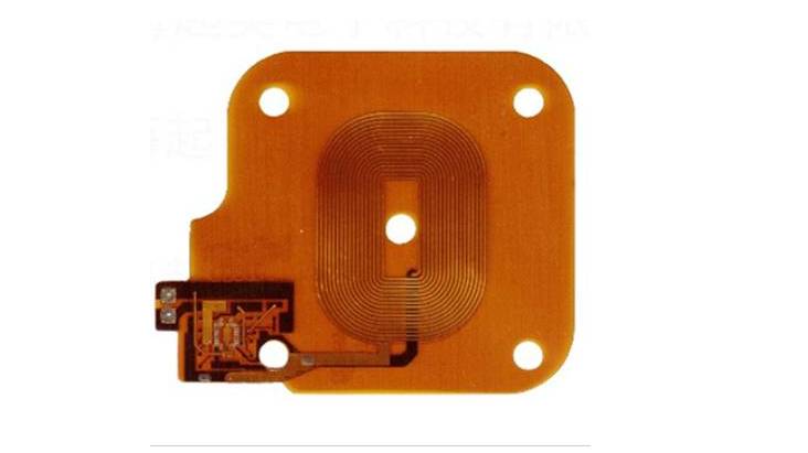
Before a flexible printed circuit board (FPCB) receives its protective coverlay, the bare substrate – typically a copper‑clad polyimide (PI) or liquid crystal polymer (LCP) laminate – must be mechanically and electrically prepared. This preparation includes:
Drilling of plated through‑holes (PTHs) and blind vias for layer‑to‑layer interconnection.
Routing (or profiling) of the outer board contour, internal slots, and mounting cutouts.
Scoring or half‑cutting for panelised arrays and bend‑relief features.
These operations are performed prior to coverlay lamination because:
The holes must be metallised (electroless copper + electrolytic plating) – a process that would be blocked or contaminated by a pre‑applied coverlay.
Routing generates debris and mechanical stresses that could delaminate or scratch a finished coverlay.
Registration for subsequent coverlay opening relies on the drilled holes as fiducials.
While mechanical drilling and CNC routing have been used for decades, the trend towards finer pitches, thinner materials, and complex 3D shapes has made laser‑based drilling and routing the dominant method in modern FPCB production.
2. Why Laser for Drilling and Routing?
Compared to conventional mechanical methods, laser processing offers decisive advantages for FPCB substrate preparation:
| Aspect | Mechanical (Carbide/Drill) | Laser |
|---|---|---|
| Minimum hole diameter | Typically ≥0.15 mm (limited by tool breakage) | Down to 25 µm (blind vias) or 50 µm (through) |
| Aspect ratio | Limited (<8:1 for small drills) | Can achieve >10:1 with tapered beams |
| Material thickness variation | Requires tool changes per thickness | Single setup, software‑adjustable |
| Wear and breakage | High tool cost, frequent replacement | No contact, no tool wear |
| Burr and smear | Produces copper burrs and resin smear (needs desmear) | Clean ablation, minimal smear (especially with UV) |
| Flexibility | Fixed tool paths, costly design changes | Digital mask‑less, quick changeover |
| Slots and complex shapes | Requires multiple passes, poor corner quality | Direct laser routing with µm‑level corner radii |
In addition, laser drilling can produce tapered via walls (positive or negative taper) which improve plating coverage, and laser routing can create stress‑relief notches and fold lines without delamination – critical for dynamic flex applications.
3. Laser Source Selection for Drilling and Routing
The choice of laser wavelength and pulse duration depends on the material stack (PI thickness, copper foil thickness, and whether copper is present on one or both sides) and the feature type (through‑hole, blind via, or contour cut).
| Laser Type | Wavelength | Pulse Width | Best Application | Key Characteristics |
|---|---|---|---|---|
| UV DPSS (355 nm) | 355 nm | Nanosecond | Drilling through copper + PI; small vias (≥50 µm); routing thin (<0.2 mm) flex | High absorption by both copper and PI; photochemical ablation; low HAZ; excellent for blind vias stopping on inner copper |
| CO₂ (9.3–10.6 µm) | ~10 µm | Microsecond | Drilling PI after copper has been removed (or copper‑free areas); routing thick PI | High absorption in PI, but reflected by copper – requires pre‑opening copper windows with UV laser; produces larger HAZ; cost‑effective for large‑diameter through‑holes (>150 µm) in PI |
| Green (532 nm) | 532 nm | ns / ps | Intermediate applications; copper removal with less back‑reflection | Better absorption in copper than IR, but less than UV; used in some cost‑sensitive UV‑green hybrid systems |
| Picosecond UV (355 nm) or IR (1064 nm) | 355 / 1064 nm | ps | High‑end blind vias in LCP or high‑frequency materials; micro‑routing with zero taper | Extremely cold ablation; no melt, no recast layer; ideal for vias with <5 µm HAZ; essential for aerospace and medical implants |
Practical recommendation: For most high‑volume FPCB drilling, a nanosecond UV laser (355 nm) is the workhorse – it drills copper and PI in one pass, produces clean sidewalls, and can be switched to routing mode with the same optics. For PI‑only drilling (after copper window opening), CO₂ lasers offer higher throughput for large holes. For cutting outer contours with minimal charring, UV is again preferred.
4. Critical Process Parameters for Drilling and Routing
4.1. For Through‑Hole Drilling
Pulse energy must be high enough to penetrate the full stack (e.g., 18 µm Cu + 25 µm PI + 18 µm Cu) – typically 100–300 µJ per pulse for 355 nm, depending on spot size.
Pulse repetition rate and trepanning speed determine the hole quality. Using a trepanning (spiral) motion instead of percussion (single‑shot) yields cleaner walls and reduces taper.
Number of passes – 2–3 passes are often used: first pass breaks through the top copper, second ablates the PI, third clears the bottom copper. This minimises copper splatter and re‑deposition.
Assist gas – air or nitrogen at 1–3 bar blows molten debris out; nitrogen prevents oxidation of the copper wall, which is critical for subsequent plating adhesion.
4.2. For Blind Via Drilling (stopping on inner copper)
End‑point detection is essential. Use a coaxial optical sensor that detects a change in plasma emission or reflected signal when the beam hits the copper bottom layer.
Fluence must be carefully tuned – too high and it damages the bottom copper (pitting); too low and it leaves PI residue.
Typically, a constant‑fluence, multi‑pass strategy with decreasing pulse energy for the final pass ensures a clean, flat copper surface.
4.3. For Routing (Contour Cutting and Slotting)
Scanning mode: Instead of trepanning, the beam follows the desired outline using a galvanometer scanner with a large field lens.
Kerf width depends on spot size and focal position. For fine routing, use a small spot (20–30 µm) and multiple overlapping passes to achieve the required width.
Cutting speed is a trade‑off with edge quality. For a 25 µm PI + 18 µm Cu stack, a typical routing speed is 200–500 mm/s with 1–2 passes.
Corner control: Apply radius compensation to avoid sharp inner corners (stress risers). Program a small fillet (≥50 µm) automatically.
5. Edge Quality and Plating Compatibility
The post‑drill surface quality directly affects the success of electroless copper deposition and subsequent electrolytic plating. Key metrics:
Roughness (Ra) – should be <1.0 µm for good adhesion; laser‑ablated surfaces are naturally micro‑rough, which is beneficial.
Smear / residue – PI ablation can leave carbonaceous residue. This can be removed by a mild plasma or permanganate desmear step, but UV laser (photochemical) produces far less smear than CO₂ (thermal).
Taper angle – a slight positive taper (top wider than bottom) improves plating coverage. This is achieved by slightly defocusing the beam or using a conical beam shaping optic.
Copper oxidation – avoid by using nitrogen assist; oxidised copper is difficult to plate and reduces solderability.
Practical test: After drilling, cross‑section the vias and inspect for cracks, micro‑cracks, or delamination between copper and PI (per IPC‑TM‑650 2.1.1). Also perform a plating coverage test – the plated copper thickness should be uniform (±20%) along the via wall.
6. Integration into the FPCB Manufacturing Workflow
The pre‑lamination laser drilling/routing step is typically positioned after circuit pattern etching and before coverlay lamination. A typical workflow:
Raw laminate (Cu/PI/Cu) → circuit imaging + etching → inner layer inspection.
Laser drilling of all via types (through, blind, buried) – using registration marks etched on the panel.
Desmear / plasma cleaning (if required) to remove residue.
Electroless copper + electrolytic plating to metallise the holes.
Outer layer imaging + etching (if multi‑layer build‑up).
Laser routing of outer contour, slots, and scoring lines.
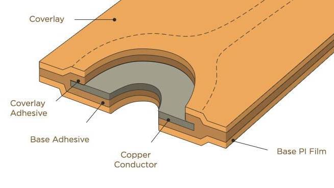
Coverlay lamination – after routing, the panel is clean and free of debris.
DFM guidelines for drilling/routing:
| Parameter | Recommendation |
|---|---|
| Minimum via diameter | ≥60 µm for through‑holes; ≥40 µm for blind vias (depending on laser) |
| Pad size | Pad diameter ≥ via diameter + 150 µm to accommodate misregistration |
| Via‑to‑via spacing | ≥200 µm (to avoid web breakage) |
| Routing kerf | Account for kerf width (typically 30–50 µm) in design – add 2× kerf to the cut line |
| Tab routing | For panelised boards, leave small tabs (0.5–1 mm) to hold the board; these are later broken off or second‑pass cut |
| Slots and cutouts | Minimum slot width = 2× kerf, but preferably ≥0.2 mm for mechanical strength |
7. Emerging Trends in Laser Drilling and Routing
Multi‑wavelength hybrid systems – combining a CO₂ laser for large PI holes and a UV laser for fine copper apertures in one machine, reducing handling time.
Real‑time hole‑by‑hole monitoring – using machine vision and AI to detect incomplete drilling and automatically re‑work on the fly.
Ultrafast lasers for LCP and high‑frequency materials – as 5G and mm‑wave applications grow, materials like LCP are sensitive to heat; picosecond lasers with <10 ps pulses are becoming standard.
Laser‑assisted chemical etching – a combined process where laser modifies the PI surface to enhance subsequent wet etching, improving throughput for extremely high‑density vias.
In‑line metrology – integrating confocal or white‑light interferometry after drilling to measure depth and diameter, feeding back to the laser controller for closed‑loop correction.
8. Quality Assurance and Defect Prevention
Common defects in pre‑lamination drilling/routing and their solutions:
| Defect | Root Cause | Mitigation |
|---|---|---|
| Over‑sized or tapered holes | Focus drift or incorrect trepanning radius | Regular focus calibration; use beam profiler; adjust trepanning offset per material lot |
| Burr / raised copper at entry | High pulse energy or insufficient overlap | Reduce fluence; increase number of passes; use helium assist gas to suppress plasma shielding |
| PI residue at bottom of blind via | Insufficient final pass energy | Perform an extra low‑energy pass; use end‑point detection to confirm clearance |
| Charring / carbonisation | Thermal laser (CO₂) or too high repetition rate | Switch to UV; reduce rep‑rate; increase scan speed; use nitrogen assist |
| Cracks along routing edge | Mechanical stress from high‑speed scanning or excessive heat | Use multiple passes with lower energy; apply pre‑heating (optional) to reduce thermal shock |
| Misalignment between front and back sides | Panel distortion or poor fiducial registration | Use double‑sided alignment with through‑fiducials; apply distortion correction software |
9. Conclusion
Selecting the appropriate laser source – UV nanosecond laser for general drilling/routing, CO₂ laser for thick PI, or picosecond laser for ultra‑fine or heat‑sensitive materials – and carefully optimising fluence, overlap, assist gas, and pass strategy will yield consistent, high‑yield results. Coupled with in‑line inspection and closed‑loop control, laser processing meets the ever‑increasing demands of miniaturisation, high frequency, and extreme environment reliability. By performing these steps before coverlay lamination, manufacturers ensure that vias are clean, platable, and accurately placed, and that the board contours are stress‑free and dimensionally stable.
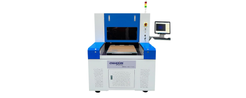
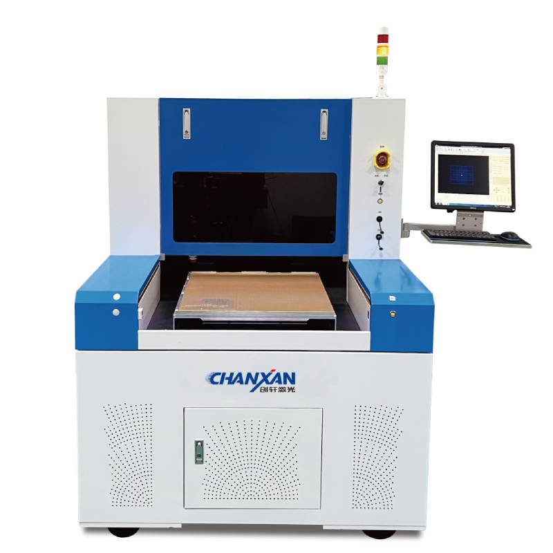
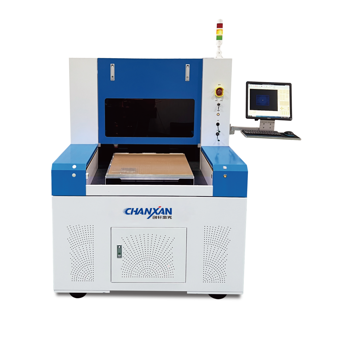
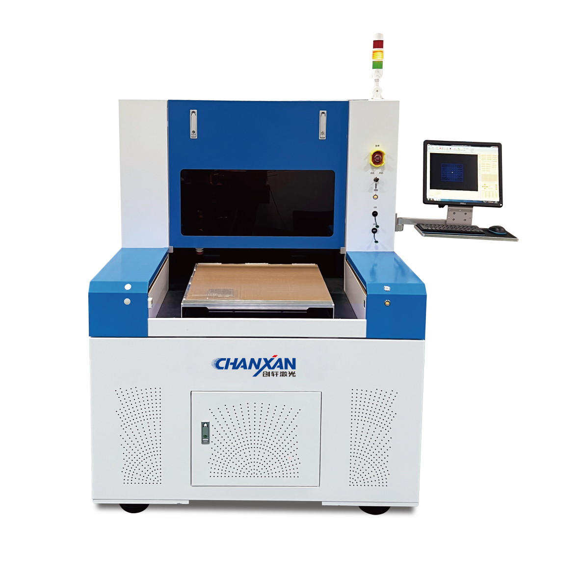
For manufacturers specifically targeting high‑precision micro‑via drilling and fine‑contour routing with minimal thermal damage, Chanxan's picosecond UV laser processing equipment is strongly recommended. Its ultra‑short pulse width (picosecond regime) delivers cold ablation with zero carbonisation, exceptional edge sharpness, and stable high‑throughput performance on advanced materials such as LCP and ultra‑thin polyimide – making it a reliable solution for next‑generation FPCB production where quality and yield are non‑negotiable.